1、扫描电子显微镜镜,简称扫描电镜,scanning electron microscope,简写SEM。
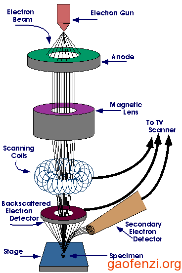
2、SEM原理:用一束极细的电子束扫描样品,在样品表面激发出次级电子,次级电子的多少与电子束入射角有关,也就是说与样品的表面结构有关,次级电子由探测体收集,并在那里被闪烁器转变为光信号,再经光电倍增管和放大器转变为电信号来控制荧光屏上电子束的强度,显示出与电子束同步的扫描图像。(来源:百度百科)
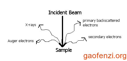
下图是电子束打在样品表面并且激发出次级电子:
The SEM is an instrument that produces a largely magnified image by using electrons instead of light to form an image. A beam of electrons is produced at the top of the microscope by an electron gun. The electron beam follows a vertical path through the microscope, which is held within a vacuum. The beam travels through electromagnetic fields and lenses, which focus the beam down toward the sample. Once the beam hits the sample, electrons and X-rays are ejected from the sample. Detectors collect these X-rays, backscattered electrons, and secondary electrons and convert them into a signal that is sent to a screen similar to a television screen. This produces the final image.
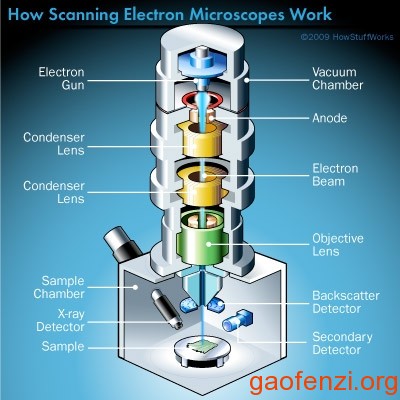
(source:purdue & howstuffworks)
3、SEM制样观察过程:取样品、干燥、粘台、喷金和观察。
4、SEM在高分子中的常见应用:
(1)观察高聚物的形态和结构;
(2)观察结晶高聚物的晶态结构;
(3)研究材料共混相容性;
(4)观察高分子纳米材料结构;
(5)表征高分子材料的降解性;
(6)研究高分子材料的生物相容性;
(7)研究多孔材料表面或断面的孔特征。
参考文献:《高分子物理近代研究方法》,第二版,张俐娜,薛奇等编著。